HABERNEWS
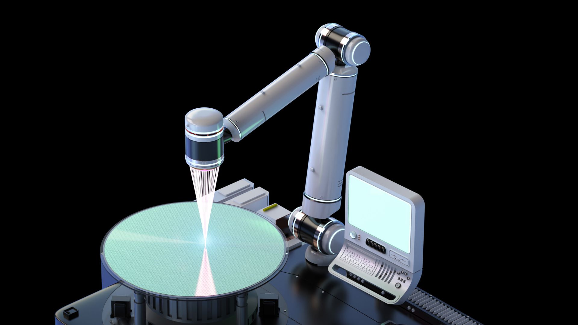 ABD'de daha yoğun çipler için yeni EUV litografi malzemeleri geliştiriliyorNew EUV lithography materials being developed in the US for higher-density chipsABD'li araştırmacılar, Berkeley Lab ve sanayi ortaklarıyla iş birliği içinde, birkaç atom ölçeğinde daha küçük ve hızlı çiplerin üretimini sağlayacak yeni EUV litografi malzemeleri üzerinde çalışıyor. Bu gelişme, ekonomik güvenlik ve ulusal savunma açısından en gelişmiş çiplere erişimi sürdürmek için kritik önem taşıyor.American researchers, in collaboration with Berkeley Lab and industry partners, are working on new EUV lithography materials that will enable the production of chips that are a few atoms smaller and faster. This development is of critical importance for maintaining access to the most advanced chips in terms of economic security and national defense. Bu, AiPulse bülteni için derlenmiş bir haber özetidir — orijinal makale değil. Orijinal haber interestingengineering.com adresinde.This is a news summary compiled for the AiPulse newsletter — not the original article. The original article is at interestingengineering.com. Orijinal haberi okuRead the original article AI Kritik →AI Critique → Türkçe (otomatik çeviri) English (automatic translation) |