 Siemens speeds up chip design with Solido Layout AnalyzerRead the article English (automatic translation) |
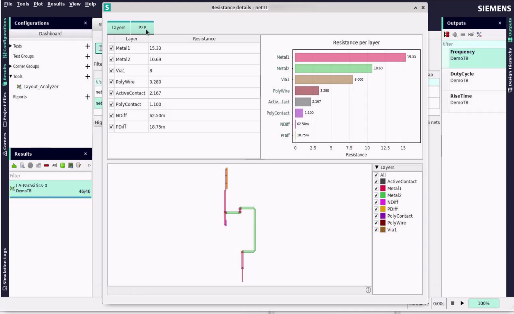
SummarySiemens introduced the Solido Layout Analyzer at DAC 2026. This post-layout analysis tool, integrated within the Solido Design Environment, directly links extracted parasitics and layout-dependent effects to circuit performance specifications using a sensitivity-based approach in the simulation loop. The tool supports Fuse, an 'agentic' interface that operates in natural language. |
Why it mattersAs transistor counts increase and layout/routing effects become increasingly dominant over device parameters in advanced nodes, late-stage parasitic cleanup can take weeks in the production cycle. A tool that automates root cause identification and scenario experimentation can shorten this bottleneck. However, the tool's true value depends on whether it performs better than existing sign-off flows, rather than merely repackaging them. |
Highlights
|
Critical takeThis is a vendor marketing piece that offers no zero-baseline benchmarks or head-to-head comparisons with existing sign-off tools. It also suspiciously vaguely defines what 'AI-assisted' means beyond a chat-style wrapper (Fuse) layered on top of sensitivity analysis and scenario simulation workflows. Until independent users publish cycle time or yield data, the 'weeks saved' claim remains an unverified promise dressed up in agentic jargon. |